 Date:2022.11.16
Visits:839
Chip yield is one of the important factors affecting the cost of enterprises. Semiconductor lasers are compound semiconductors, whose main materials are very brittle gallium arsenide and indium phosphide. In each process of its preparation, low yield is a common problem. Take foreign well-known chip enterprises as an example, their production can reach a yield of more than 70%, but the subsequent packaging and strict judgment standards for final products have accumulated a yield loss of 30%. If the yield rate is not high, special testing equipment is required to screen the defective products. In China, the bar bar test has been used at the low end of this field, and the chip after bar bar test needs secondary splitting. Various factors in the middle link will cause 3-5% yield loss for demanding high-end chips. With the increasing speed of semiconductor laser chips, there is a trend of smaller chip size and more complex process in the post packaging. These secondary damaged chips are used as good products in the post packaging process, which will bring huge cost expenditure, thus increasing the production cost of finished devices. In addition, the semiconductor laser chip is very sensitive to temperature. Because the contact of the bar bar on the test bench cannot fully meet the requirements of the chip for heat dissipation under high temperature testing conditions, repeated testing of GRR cannot be guaranteed. Therefore, domestic and foreign manufacturers have gradually shifted from low-end Bar bar testing to high-end bare Die semiconductor laser chip testing.
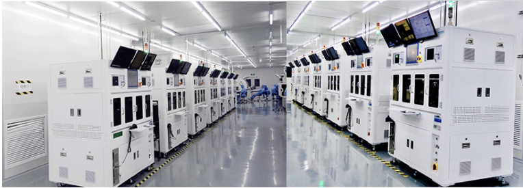
Semight Chip Tester
The laser chip tester of
Semight
is a key core high-end equipment for optical chip testing. It is a complex system integrating optical, mechanical, electrical, software and computing. Through integrated chip ID scanning, loading, transportation, high/low temperature control, testing, unloading, sorting and classification function units, it can be used to detect, judge and sort the photoelectric characteristics of different types of semiconductor lasers (DFB, EML, EML+SOA), bare Die chips and CoC chips.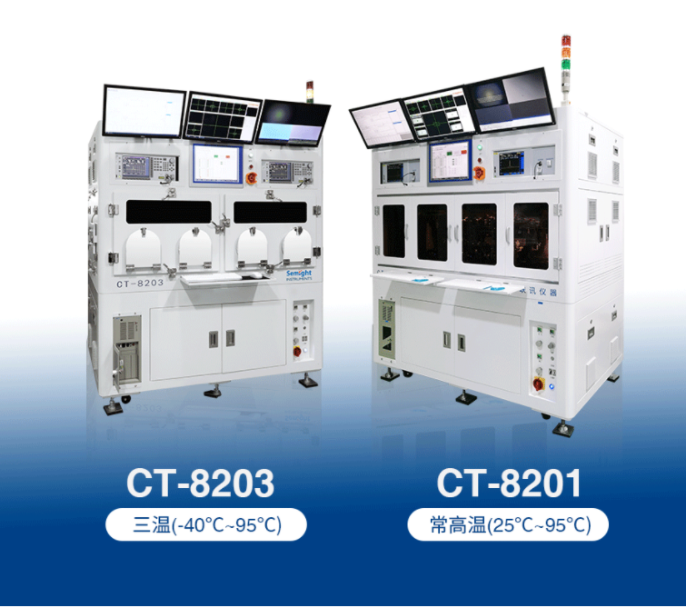
Product advantages
Supporting industrial low temperature - 40 ℃~95 ℃;
▌ Support multiple products DFB/EML/EML+SOA;
▌ Fast test speed;
▌ Patent test platform;
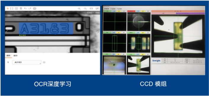
▌ OCR depth learning algorithm;
▌ High reliability and stability;
▌ Different lasers are equipped with different numbers of powered probes;
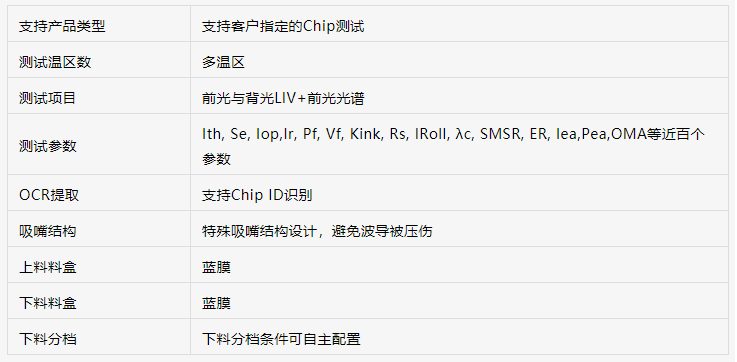
▌Support LIV scanning test of laser front light and backlight, and front light spectrum test;
Functional module of chip tester system
▌Feeding module
Support blue film or Gelpak;
Perform Die positioning and automatic calculation of adjacent material spacing within the effective range, and adjust the material position in real time
▌Chip handling module
The handling module is composed of a suction nozzle high-precision linear motor;
Realize the transfer of feeding blue film ->normal high temperature test platform ->unloading blue film
▌Visual positioning module
Visual localization and OCR extraction (OCR depth learning algorithm)
▌Test Module
Self developed temperature control platform, high thermal conductivity, high stability, and high wear resistance
Power on probe, self-developed highly reliable probe assembly, to ensure the stability of the needle
Vision+motion module, correct chip position and light angle
Large area detector and special optical collimator assembly, LIV scanning and spectral scanning test

▌Blanking and grading module
Support multiple Bin conditions, which can be configured freely
systems software
▌Powerful and simple operation
Operation interface, information input, and test plan configuration;
Test information interface, test data and test results display
Test index
▌system function
▌Optical parameters

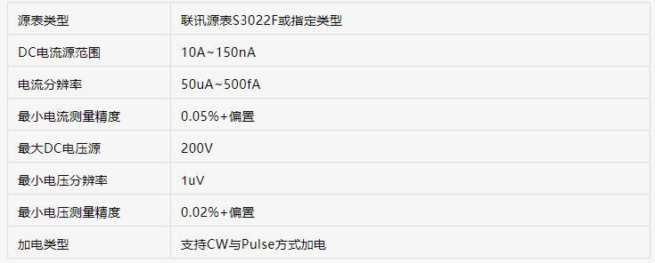
▌Electrical parameters
Large scale application
Service hotline
Follow
Name
Email verfication code
Phone
Password
Confirm Password
e-mail address
Email verification code
New Password
Confirm Password