
Wafer Level Burn-In
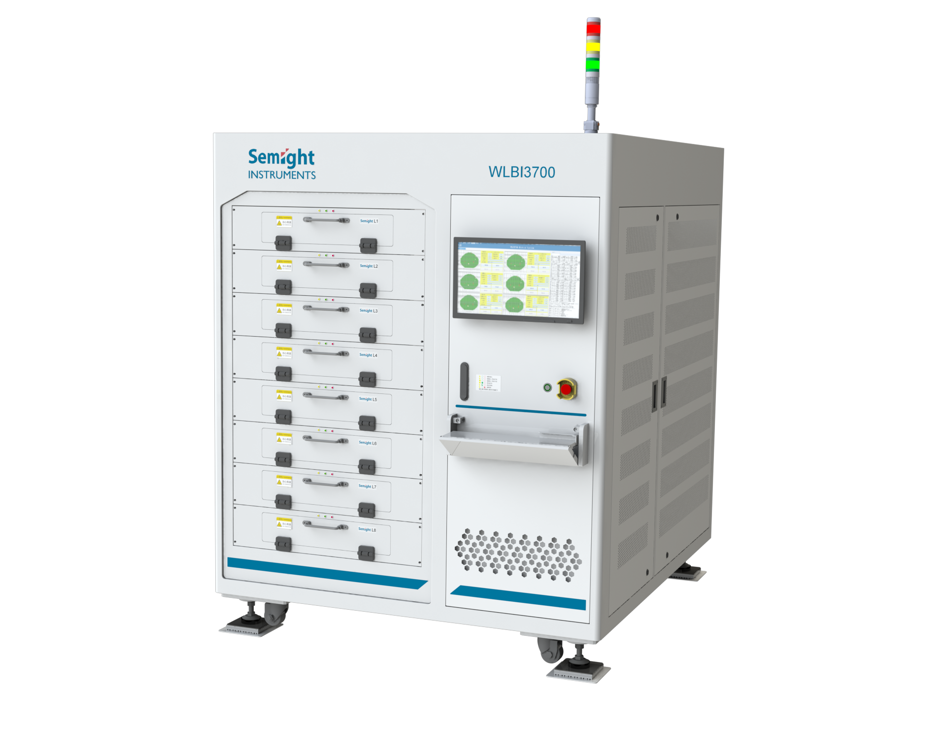
WLBI3700
HTGB Wafer Burn-In System
Semight Instrument SiC Wafer burn-in System WLBI3700 can be configured with 8 burn-in layers at most, each burn-in layer supports 6 & 8-inch wafers, the HTGB burn-in for a maximum of 1500 products performed for each wafer, it supports Igss and Vth tests in the system and can be widely used in the testing and research fields of power semiconductor characteristics, GaN and SiC characterization, composite materials, wafer technology, etc.
Feature

Also supports HTGB
Compared with GB & RB compatibility, this has a higher capacity
Multiple test functions
Support parameter test Lgss, Igss, Vth.
Real time monitoring of gate current
Timely discover product abnormalities and record data in case of abnormalities
The minimum current measurement resolution can reach 0.1 nA
Accurate measurement of leakage current
High temperature resistant design
Heating components and fixtures are high temperature resistant to meet 175°C aging requirements.
Support nitrogen protection
Prevents oxidation of PAD
Product abnormal protection function
With gate protection circuit, the output can be closed in case of short circuit
Heating power and temperature control accuracy
120 to 175 ℃: Uniformity ±3 ℃, the accuracy <1°C, and the resolution is 0.1°C.Functions and advantages
The fixture consists of two main parts: Chuck and Probe card. Fixture support a 6-inch wafer or an 8-inch wafer.
The Probe card is equipped with a Pogo Pin that meets the number of die channels on the wafer. The life of the Pogo Pin is 100,000 cycle times, the temperature resistance is 175 degrees, and the positioning accuracy is ±25um.
Chuck outer frame seal pressure keeping design, the maximum pressure keeping 0.4mPa, to prevent high temperature oxidation. There are two temperature sensors in the Chuck, one for temperature control and the other for temperature protection monitoring.Layer design
Each layer aging system can operate independently, with 12 relay boards and 12 current acquisition boards to meet 1500CH wafer aging. Each channel circuit supports protection, when there is a die short circuit failure, it can protect the safety of the circuit, but also protect the near product from being affected.
Overall design
The whole machine is consists of aging layer part and electrical part. Placed on the left side of the rack, 8 layers are placed respectively. The right side of the rack is an electrical box. Each layer has an independent electrical box, which supports independent operation of each layer.
Gate voltmeter specification |
|||
| Voltage setting accuracy | Range | Set resolution | Accuracy (1 year) ± (% reading + offset) |
| ±70 V | 10 mV | 0.1%+0.2 V | |
| ±20 V | 5 mV | 0.1%+0.1 V | |
| Overshoot | <1% (typical value) | ||
| Total power | 30 W | ||
Number of channels |
1 (each burn-in layer) |
||
Gate voltmeter specification |
|||
Voltmeter display accuracy |
Range | Display resolution | Accuracy (1 year) ± (% reading + offset) |
| ±70 V | 10 mV | 0.1%+0.2 V | |
| ±20 V | 5 mV | 0.1%+0.1 V | |
| Number of channels | 1 (each burn-in layer) |
||
Gate ammeter specification |
|||
| Current display accuracy | Range | Display resolution | Accuracy (1 year) ± (% reading + offset) |
| 10 µA | 500 pA | 0.1% + 50 nA | |
| 1 µA | 50 pA | 0.1% + 5 nA | |
| 100 nA | 10 pA | 0.1% + 0.5 nA | |
Number of channels |
12 channels (125 channels for one board) | ||
Similar recommendation
Optical communication network plays an important role in the rapid development of big data, cloud computing, 5G communication and other markets.
Semight Instruments offers various of instruments for optical Transceiver/Component testing, including wide bandwidth sampling oscilloscope, NRZ/PAM4 bit error ratio tester , burst error ratio tester, fast wavelength meter, optical spectrum analyzer, high precise source measure unit, 400G network analyzer ,optical power meter, optical attenuator, optical switch etc. Provide cost-effective complete solutions.
The high-precision source meter integrates the functions of voltage source, current source, voltmeter, ampere meter, and electronic load in one, which is widely used in high-precision IV test and measurement for various discrete components, photovoltaic, new energy, battery and other industries. Semight Instrument provides high-precision benchtop source meters and plug-in PXIe source meter modules of standard PXIe chassis, fully meeting the application of various test scenarios.
Details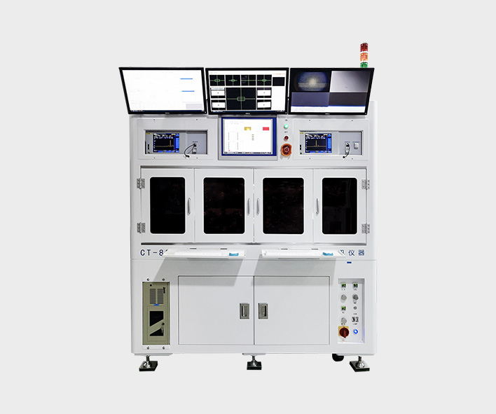
Burn-in testing of laser is an important method to ensure the reliability of laser. Through the test of COC or bare die, the early failure of laser caused by the defects in the process of laser production can be screened out in advance. Semight Instrument provides a complete solution from bare die to COC, from high temperature(150℃ or higher) to low temperature (-40℃), with CoC automatic loading and unloading system, forming a complete test solution, Semight Instrument's laser chip burn-in/load/unload test system has been widely recognized by the market.
Details
The semiconductor front-end test is mainly used in the wafer processing to check whether the processing parameters of the wafer products meet the design requirements or there are defects affecting the yield after each step of the manufacturing process. The semiconductor back-end test equipment is mainly used after wafer processing to check whether the performance of the chip meets the requirements, which belongs to the electrical performance test. Semight Instrument provide integrated solutions such as wafer burn in and known good die tester, improve test efficiency and reduce test cost.
Detailsmailbox
Service hotline
follow
full name
e-mail address
Email verification code
Telephone
password
Confirm Password
e-mail address
Email verification code
New Password
Confirm Password
 Apply for prototype