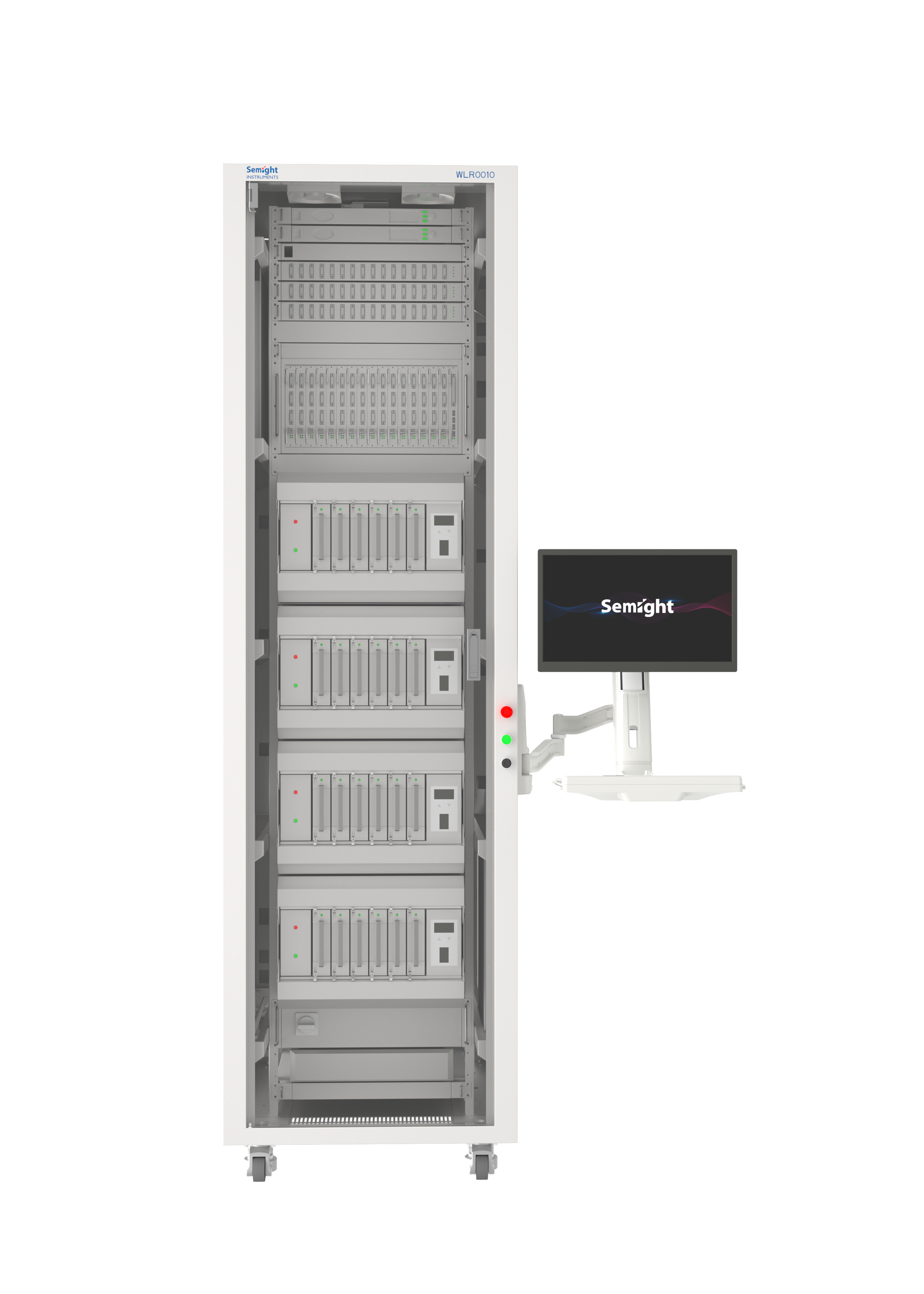

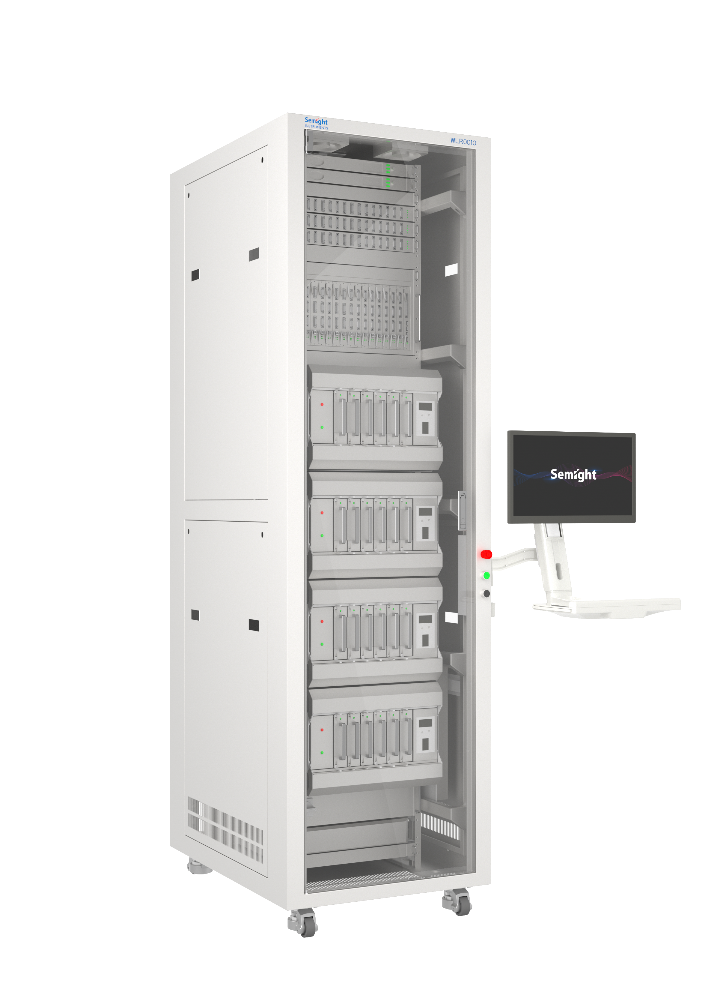

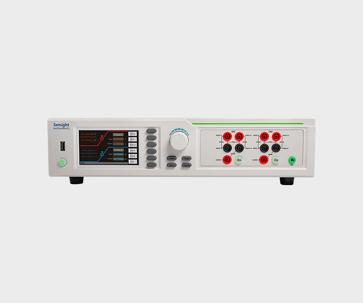
Wafer Level Reliability
WLR0010
High temperature electrification reliability testing system
The wafer level reliability testing system WLR0010 is a high-temperature electrification reliability testing system for semiconductor crystal properties. The product is based on The JEDEC standard enables fast violation testing of the reliability of gate oxide layers in devices, while greatly reducing testing cycles and costs through multimode and high parallel measurements.
Features

Supports high-voltage testing
up to 3500V
High parallel measurement
up to 768 DUTs
Automatic switching of testing modes through multi-channel measurement

Support wafer level and package level testing
Platform unification
Support JEDEC device reliability testing standards
32 channels
Supports On the fly testing
and data analysis software
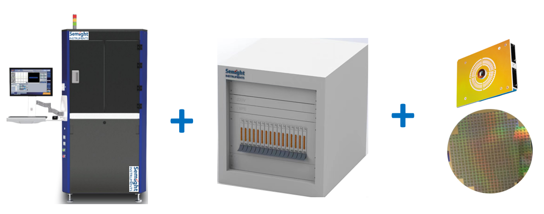
Support for different packaging devices
By replacing the Board and wafer probe cards
Adjustable temperature and electrical stress
Features and Benefits
Technical Indicators
|
Test Item |
TDDB/HCI/NBTI/EM |
|
|
Parallel measurement quantity (maximum) |
PLR |
768 DUTs |
|
WLR |
16 Sites Multi-site |
|
|
Single plate source |
30 Source |
|
|
Voltage |
±(20V~3500V) |
|
|
Voltage accuracy |
±20V |
0.2%RD±5mV |
|
±200V |
0.2%RD±50mV |
|
|
±2000 V |
0.2%RD±200mV |
|
|
±3500 V |
0.2%RD±300mV |
|
|
Voltage resolution |
10 μV |
|
|
Current accuracy |
10mA~100mA |
0.2%RD±500μA |
|
1mA~10mA |
0.2%RD±50μA |
|
|
100μA~1mA |
0.2%RD±500nA |
|
|
10μA~100μA |
0.2%RD±50nA |
|
|
1μA~10μA |
0.2%RD±5nA |
|
|
100nA~1μA |
0.2%RD±500pA |
|
|
10nA~100nA |
0.2%RD±50pA |
|
|
1nA~10nA |
0.2%RD±5pA |
|
|
10pA~1nA |
0.2%RD±200fA |
|
|
Current resolution |
10 fA |
|
|
Temperature Range |
(RT+10℃)~+200℃ (TDDB/HCI/NBTI) |
|
|
Other |
Support On-the-fly Test Support Vth Scan:0~200V Support Vramp Test Over Voltage/Current monitor |
|
Accuracy measurement conditions: temperature 23 ± 5 degrees, humidity 35% -60%, system operation time 1 hour, integration time LONG (below 1nA)
|
voltage source/Ichimoku Kinko Hyo |
|||||
|
voltage accuracy |
Range |
Resolution ratio |
Precision(1year) ±(%reading+polarization) |
Pink noise(effective value) 0.1 Hz-10Hz |
|
|
High-voltage power supply |
±3500 V |
40 mV |
0.02%+600 mV |
50 mV |
|
|
±1500 V |
20 mV |
0.02%+300 mV |
25 mV |
||
|
±600 V |
7mV |
0.02%+120 mV |
10 mV |
||
|
Low-pressure source |
±200 V |
100 μV |
0.02% + 40 mV |
1mV |
|
|
±20 V |
10 μV |
0.02% + 5 mV |
200μV |
||
|
±6 V |
1 μV |
0.02% + 500 μV |
60μV |
||
|
Temperature coefficient |
±(0.15 × precision index)/°C (0℃-18℃,28℃-50℃) |
||||
|
Set time |
<±1% (typical value Normal,Step is the range 10% to 90%,Full scale point, resistive load test) |
||||
|
Overshoot |
<±0.1%(Typical values, full scale points, resistive load tests) |
||||
|
current source/Table pointer |
||||
|
Current accuracy |
Range |
Resolution ratio |
Precision(1 year) ±(%reading+polarization) |
Typical noise(effective value) 0.1 Hz-10Hz |
|
±15 mA |
10 nA |
0.02% +2 μA |
±15 mA |
|
|
±1.5 mA |
1 nA |
0.2% + 150 nA |
±1.5 mA |
|
|
±150 μA |
100 pA |
0.2% + 20 nA |
±150 μA |
|
|
±15 μA |
10 pA |
0.2% +3 nA |
±15 μA |
|
|
±1.5 μA |
1 pA |
0.3% + 600 pA |
±1.5 μA |
|
|
±150 nA |
100fA |
0.5% + 300 pA |
±150 nA |
|
|
±10 nA |
10 fA |
0.5% + 5 pA |
1 pA |
|
|
Temperature coefficient |
±(0.15×precision index)/°C(0℃-18℃,28℃-50℃) |
|||
|
Set time |
<±1% (Typical value,Normal,The step is range10%to90%) |
|||
|
Overshoot |
<±0.1%(Typical values, full scale points, resistive load tests) |
|||
Similar recommendation
Optical communication network plays an important role in the rapid development of big data, cloud computing, 5G communication and other markets.
Semight Instruments offers various of instruments for optical Transceiver/Component testing, including wide bandwidth sampling oscilloscope, NRZ/PAM4 bit error ratio tester , burst error ratio tester, fast wavelength meter, optical spectrum analyzer, high precise source measure unit, 400G network analyzer ,optical power meter, optical attenuator, optical switch etc. Provide cost-effective complete solutions.
The high-precision source meter integrates the functions of voltage source, current source, voltmeter, ampere meter, and electronic load in one, which is widely used in high-precision IV test and measurement for various discrete components, photovoltaic, new energy, battery and other industries. Semight Instrument provides high-precision benchtop source meters and plug-in PXIe source meter modules of standard PXIe chassis, fully meeting the application of various test scenarios.
Details
Burn-in testing of laser is an important method to ensure the reliability of laser. Through the test of COC or bare die, the early failure of laser caused by the defects in the process of laser production can be screened out in advance. Semight Instrument provides a complete solution from bare die to COC, from high temperature(150℃ or higher) to low temperature (-40℃), with CoC automatic loading and unloading system, forming a complete test solution, Semight Instrument's laser chip burn-in/load/unload test system has been widely recognized by the market.
Details
The semiconductor front-end test is mainly used in the wafer processing to check whether the processing parameters of the wafer products meet the design requirements or there are defects affecting the yield after each step of the manufacturing process. The semiconductor back-end test equipment is mainly used after wafer processing to check whether the performance of the chip meets the requirements, which belongs to the electrical performance test. Semight Instrument provide integrated solutions such as wafer burn in and known good die tester, improve test efficiency and reduce test cost.
Detailsmailbox
Service hotline
follow
full name
e-mail address
Email verification code
Telephone
password
Confirm Password
e-mail address
Email verification code
New Password
Confirm Password
 Apply for prototype