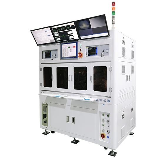
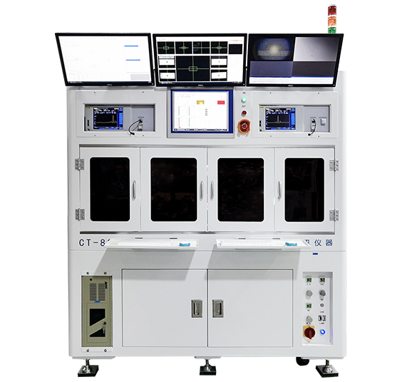
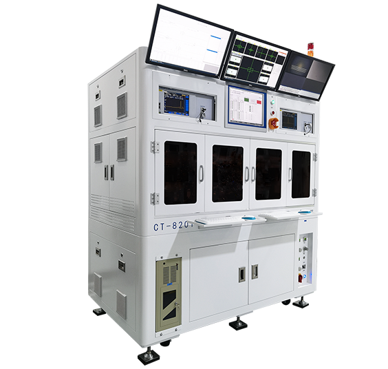

Laser Diode Test
CT8201
RT & HT Die tester
Features

Fully automated and intelligent integrated solutions
Highly integrated and fully automated solution covering very complex testing processes
High efficiency
Improve efficiency and reduce potential risks of human involvement
Maintenance and upgrades are very simple
All mechanical parts can be returned to the factory independently
Easy to use
Automatic alarm status and prompt display,Features and Benefits
Fully automated and intelligent integrated solutions
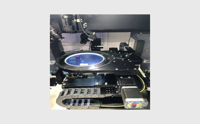
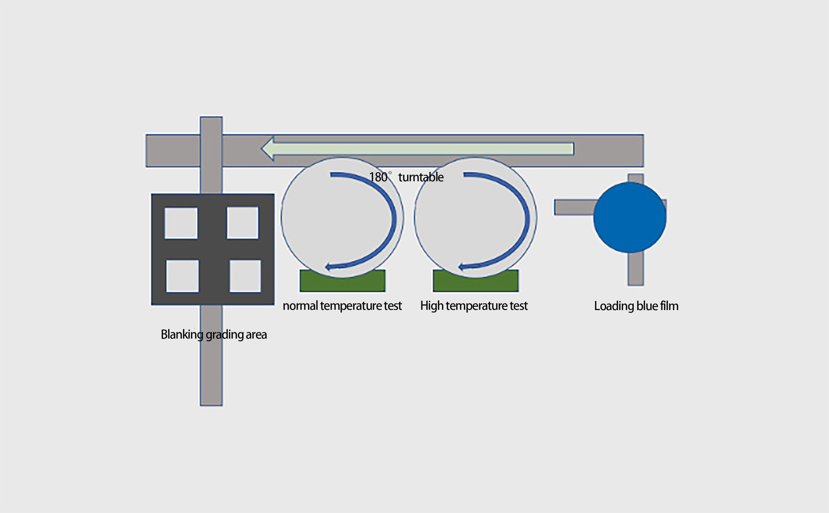
Loading module
This module consists of thimble Z module, X/Y motion module, and blue film rotation module 4 sub-function modules. Pickup function.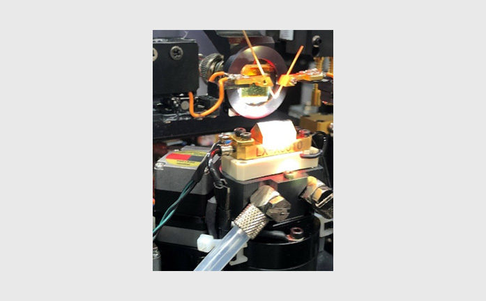
High temperature and normal temperature test module
This module consists of a hollow rotating platform, two 3-axis chip calibration modules on the front and back, and a 3-axis light detection module, with an ID/position recognition camera above the module, and Power on the probe to adjust the module, complete the calibration of the position and angle after feeding, and power on the chip test. The PD/collimator uses a motion axis for fast switching of functions.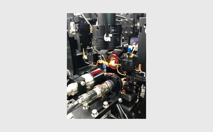
Camera and probe power-on module
The loading camera on the right side of the device is matched with the loading module to complete the loading recognition function of the Chip (different functional components can be matched according to the requirements of incoming materials) The camera above the high/normal temperature test module (in the middle of the device), after the chip feeding action is completed, the position calibration of the chip is completed by taking multiple pictures with the 3-axis motion module (the high temperature camera synchronously completes the ID identification of the chip).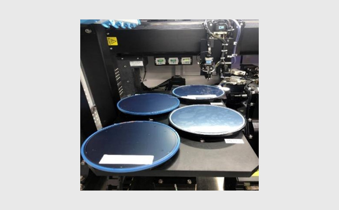
Blanking binning module
The blanking module is equipped with 4 tray placement areas, which can support 4,6-inch blue films, Or customize compatible unloading carriers according to customer needs.| Parameter Type | Parameter name | Parameter index |
| System parameters | Chip type | Support DFB, EML and EML+SOA chips |
| Chip size | L&W≥150 μm, H≥80~150 μm | |
Test Seats |
2 | |
| Test items | Front/back IL, WL | |
| Test parameters | Ith, Se, Iop, Pf, Vf, Kink, Rs, IRoll, λc, SMSR etc. | |
| OCR | Auto OCR |
|
| Nip | Specially designed suction nozzle structure, first peeled from the material box, and then sucked up | |
Loading Container |
1 6-inch blue tap |
|
Unloading Container | 4 6-inch blue taps |
|
Sorting |
Support any requirements customer need |
|
| Standard sample control | The software supports the standard sample control function. If the standard sample is tested on the local machine unit exceeding the time cycle (configurable), the system will automatically give an alarm | |
| Test configuration control | The software supports test configuration control, including test instruments, test algorithms, test sequences, test results judgment, etc. | |
| Test Data | Support all test data requested by users/support MES related requirements | |
| Electrical indicators | SMU Type | Semight self-developed SMU or other specified types |
DC Current |
3 A | |
| I/V source resolution | 10 fA/100 nV | |
| I/V Measurement resolution | 10fA/100nV Minimum Supply Resolution (6½ digits) | |
| Voltage range | 70 V | |
| Pulse current | 10 A | |
| Overcharge under normal operating | No EOS | |
| Under normal operating | No EOS | |
Overshoot under Abnormal Operation |
No EOS | |
Undershoot under Abnormal Operation |
No EOS | |
| Optical index | Detector Type | Ge |
| Wavelength range | 800~1700 nm | |
| Optical power measurement range | 10 μW-25 mW(>25 mW with attenuation plate ) | |
| Optical power measurement accuracy | 0.1 dB | |
Optical Spectrum Range |
1250-1650 nm (850 is an option) | |
Optical Spectrum Accuracy |
0.1nm | |
| Power coupling efficiency | Coupled power >-15 dBm | |
| 0.2 dB | ||
| Temperature control index | Temperature control method | TEC |
| Temperature range |
25~95 ℃ |
|
| Temperature zone | 40 ℃/min | |
| Temperature drop rate | 2 independent temperature control zones (dual stage) | |
Ramp up speed |
40 ℃/min | |
Ramp down speed |
40 °C/min | |
| Temperature accuracy | ±0.5 ℃ | |
| Temperature stability | ±0.2 ℃ | |
System Parameter |
Ith Repeatability | ±1% |
| Power repeatability | ±2% | |
| Wavelength repeatability | <±0.2 nm | |
| SMSR Repeatability | <3 dB | |
| OCR success rate | 99% | |
| Test time | <6s to finish all operations, including loading, OCR, 1 times LIV, 3 times Spectrum, unloading and sorting |
Similar recommendation
Optical communication network plays an important role in the rapid development of big data, cloud computing, 5G communication and other markets.
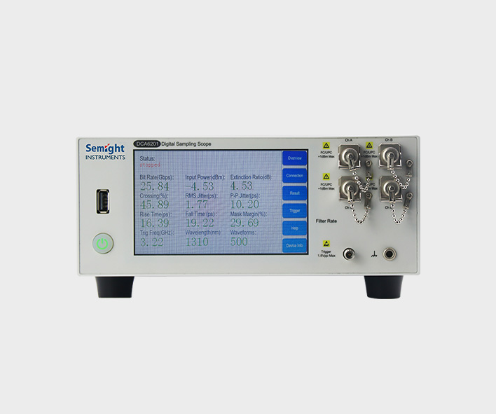
Semight Instruments offers various of instruments for optical Transceiver/Component testing, including wide bandwidth sampling oscilloscope, NRZ/PAM4 bit error ratio tester , burst error ratio tester, fast wavelength meter, optical spectrum analyzer, high precise source measure unit, 400G network analyzer ,optical power meter, optical attenuator, optical switch etc. Provide cost-effective complete solutions.
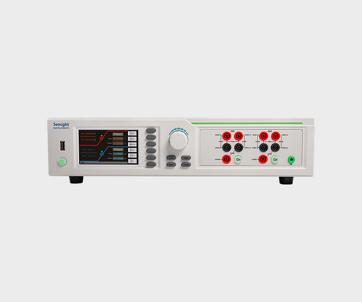
The high-precision source meter integrates the functions of voltage source, current source, voltmeter, ampere meter, and electronic load in one, which is widely used in high-precision IV test and measurement for various discrete components, photovoltaic, new energy, battery and other industries. Semight Instrument provides high-precision benchtop source meters and plug-in PXIe source meter modules of standard PXIe chassis, fully meeting the application of various test scenarios.
Details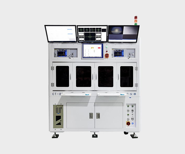
Burn-in testing of laser is an important method to ensure the reliability of laser. Through the test of COC or bare die, the early failure of laser caused by the defects in the process of laser production can be screened out in advance. Semight Instrument provides a complete solution from bare die to COC, from high temperature(150℃ or higher) to low temperature (-40℃), with CoC automatic loading and unloading system, forming a complete test solution, Semight Instrument's laser chip burn-in/load/unload test system has been widely recognized by the market.
Details
The semiconductor front-end test is mainly used in the wafer processing to check whether the processing parameters of the wafer products meet the design requirements or there are defects affecting the yield after each step of the manufacturing process. The semiconductor back-end test equipment is mainly used after wafer processing to check whether the performance of the chip meets the requirements, which belongs to the electrical performance test. Semight Instrument provide integrated solutions such as wafer burn in and known good die tester, improve test efficiency and reduce test cost.
Detailsmailbox
Service hotline
follow
full name
e-mail address
Email verification code
Telephone
password
Confirm Password
e-mail address
Email verification code
New Password
Confirm Password
 Datasheet
 Apply for prototype