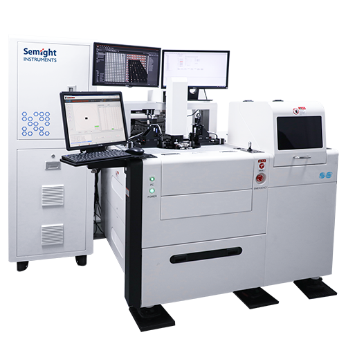

Silicon Photonics
sCT9001
SiPh Wafer Test System
Feature

Automatic/Semi-automatic
Support automatic and semi-automatic wafer loading and unloading
Wafer size
Supports 8-inch and 6-inch waferss(4- and 12-inch can be customized)
Test temperature
Support the test temperature range from room temperature to 150 ℃ (other temperatures can be customized)
Test function
Support optical-optical test, photoelectric test and electrical parameter test
DC/AC
Support DC and AC test
Grating vertical coupling
Grating coupling, FA coupling, and edge coupling
High efficiency
For different types of chips, support rapid replacement of different types of pin cards
Software function
The software supports the addition of customer database and MES functionsFunctions and advantages
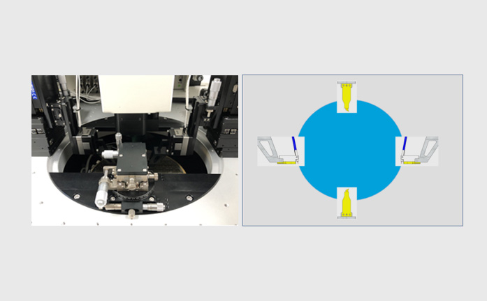
High accuracy probe station:
Wafer loading mode supports fully automatic mode and semi-automatic mode operation, which is suitable for laboratory verification and mass production;
The fully closed-loop high-accuracy motion control system is provided with automatic accuracy compensation function and its positioning accuracy is up to 3um;
The special mechanism design and calibration system can make the wafer on chuck have better planarity and better perpendicularity in Z direction of probe;
A high-definition zooming CCD configured on the system can make the power on PAD clearly visible and display low-magnification and high-magnification multi-view screens at the same time;
The built-in integrated shock-proof design is adopted which can isolate the external vibration and ensure a good test stability;
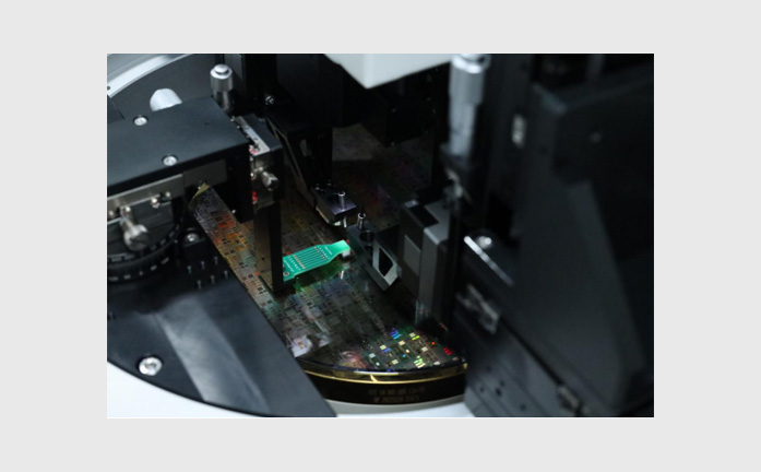
Coupling test module:
The coupling test module includes coupling optical probe, DC probe and RF probe;
The optical probe supports single-channel coupling and dual-channel coupling;
The optical probe is provided with a high-precision altimeter to ensure the consistency of the height from the incident fiber end face to the chip surface between different chips;
The optical fiber coupling module is composed of a three-dimensional lead screw motor matched with a three-dimensional high-precision piezoelectric ceramic module to ensure the optical coupling efficiency and the optical coupling repeatability;
The standard high-precision coupling controller configured on the system which can help the system realize the functions of fully closed-loop control and hardware synchronization improve the coupling accuracy and coupling speed;
The design of the probe card holder is more convenient for the replacement of the probe card, which is convenient to quickly replace the probe card for different products or different test items;
Test parameters
|
Parameter Type |
Test Parameters |
Parameter Indicators |
Definition |
|
O/O |
Insert Loss |
dB/cm |
Insert transmission loss |
|
Coupling Strength |
% |
Coupling efficiency, the ratio of the optical power received by the DUT to the incident optical power |
|
|
Polarization Dependent Loss |
dB |
Polarization-dependent loss refers to the ratio of the maximum power to the minimum power after different polarization states pass through the DUT when the polarization state of the transmitted optical signal changes in all polarization states. |
|
|
Wavelength Scan |
dBm |
Full wavelength scanning |
|
|
3dB bandwidth |
Hz |
3dB bandwidth test |
|
|
O/E |
PD Responsivity |
A/W |
PD responsivity, the efficiency of PD detector converting the received light into current |
|
Modulator ER |
dB |
Static extinction ratio, the ratio of the maximum value to the minimum value of the optical power absorbed by the modulator under different bias voltages |
|
|
E/E |
PD Dark Current |
nA |
PD dark current, the feedback current measured by increasing the bias voltage to the PD under no-light conditions |
|
Heat Resistance |
Ω |
Thermal impedance |
System test indicator
|
No. |
Specification |
Indicator |
|
1 |
Support wafer size |
6-inch ~ 8-inch (customization: 4-inch, 12-inch ) |
|
2 |
Temperature range |
RT~150℃ |
|
3 |
Temperature uniformity |
<±0.5℃ |
|
4 |
25℃→150℃ |
<15 mins |
|
5 |
150℃→25℃ |
<30 mins (manual station) |
|
6 |
Loading and unloading method |
Automatic and manual |
|
7 |
Single coupling time |
<2s (spiral trajectory length <300μm) |
|
8 |
Coupling repetition difference |
<0.2dB (individual channel) |
|
9 |
Test type |
DC test, which can be upgraded to support AC |
|
10 |
Test items |
O/O,O/E,E/E |
|
11 |
Bandwidth test deviation |
<1.5G |
|
12 |
Wafer Map function |
It can be edited, can automatically generate Map and display each Die coordinate |
|
13 |
Sub-Bin function |
It supports sub-Bin function, can distinguish test results by multiple colors and display the number and proportion of different colors |
|
14 |
Automatic needle cleaning function |
Support |
|
15 |
CCD auto-focus function |
Support |
|
16 |
Camera monitoring screen |
Support low-magnification and high-magnification multi-view screens |
|
17 |
EMI shielding |
>20dB @1KHz-1MHz |
|
18 |
Spectral noise basement |
≦150dBVrms/rtHz(≦1MHz) |
|
19 |
System AC noise |
≦15mVp-p(≦1GHz) |
Similar recommendation
Optical communication network plays an important role in the rapid development of big data, cloud computing, 5G communication and other markets.
Semight Instruments offers various of instruments for optical Transceiver/Component testing, including wide bandwidth sampling oscilloscope, NRZ/PAM4 bit error ratio tester , burst error ratio tester, fast wavelength meter, optical spectrum analyzer, high precise source measure unit, 400G network analyzer ,optical power meter, optical attenuator, optical switch etc. Provide cost-effective complete solutions.
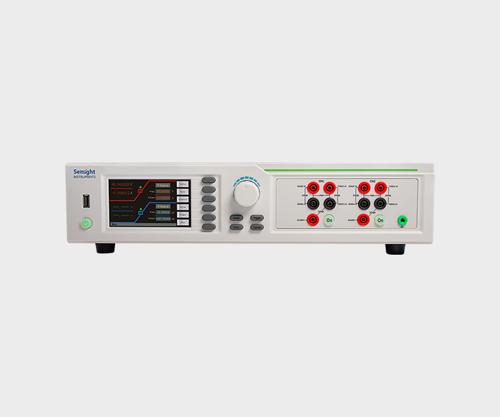
The high-precision source meter integrates the functions of voltage source, current source, voltmeter, ampere meter, and electronic load in one, which is widely used in high-precision IV test and measurement for various discrete components, photovoltaic, new energy, battery and other industries. Semight Instrument provides high-precision benchtop source meters and plug-in PXIe source meter modules of standard PXIe chassis, fully meeting the application of various test scenarios.
Details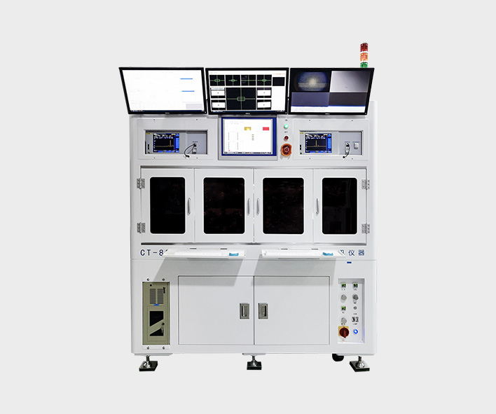
Burn-in testing of laser is an important method to ensure the reliability of laser. Through the test of COC or bare die, the early failure of laser caused by the defects in the process of laser production can be screened out in advance. Semight Instrument provides a complete solution from bare die to COC, from high temperature(150℃ or higher) to low temperature (-40℃), with CoC automatic loading and unloading system, forming a complete test solution, Semight Instrument's laser chip burn-in/load/unload test system has been widely recognized by the market.
Details
The semiconductor front-end test is mainly used in the wafer processing to check whether the processing parameters of the wafer products meet the design requirements or there are defects affecting the yield after each step of the manufacturing process. The semiconductor back-end test equipment is mainly used after wafer processing to check whether the performance of the chip meets the requirements, which belongs to the electrical performance test. Semight Instrument provide integrated solutions such as wafer burn in and known good die tester, improve test efficiency and reduce test cost.
Detailsmailbox
Service hotline
follow
full name
e-mail address
Email verification code
Telephone
password
Confirm Password
e-mail address
Email verification code
New Password
Confirm Password
 Datasheet
 Apply for prototype